
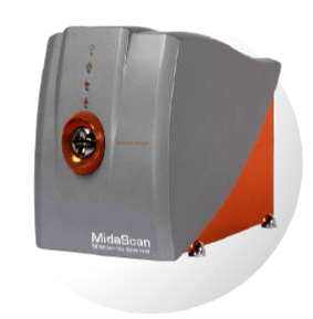
MidaScan & MidaScan-IR 雙頻增強螢光影像系統 MidaScan與MidaScan-IR提供大面積高感度的共軛焦螢光影像,其中MidaScan為Cy3與Cy5雙頻率偵測系統,MidaScan-IR為700nm與800nm雙頻率偵測系統,適用於快速細胞與組織螢光成像。 產品特色: - 使用一般螢光染劑,搭配pGOLDTM訊號增益基板,可將螢光訊號放大5 – 100 倍,只需極微量的樣品(< 5 ul)即可有效量測。 - 可偵測極小樣品體積試樣,接近 1-10um 之血清血液 - 近單分子程度影像分析 - 高效益快速篩選與 in vitro 診斷 - 大面積的影像偵測範圍,可在一片基板上同時量測14組樣品,每組樣品10 – 20個生物標記。 - 應用範圍: 螢光增強 DNA/蛋白質/抗體/細胞之檢測 產品型錄下載
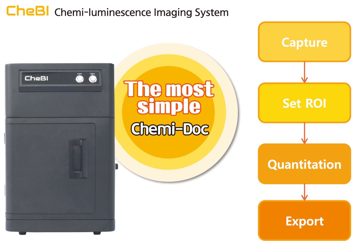
蛋白質檢測 You don’t need darkroom for Western blotting anymore!! 產品規格
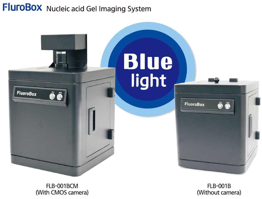
使用470nm LED激發光源,搭配NEOgreen染色劑,無需使用傳統EtBr。軟體操作簡單,可進行定量分析。機體輕巧不占空間,雙邊可開式側門,增加操作便利性。 產品規格
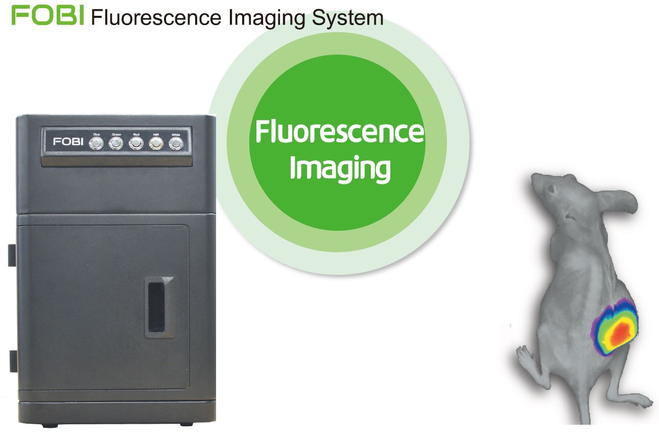
操作簡單,只需一個按鍵即可量測 專屬操作軟體,可扣除背景,亦可進行定量分析 體積輕巧(260 × 260 × 400mm),不占空間 高性能且價格實惠 產品規格
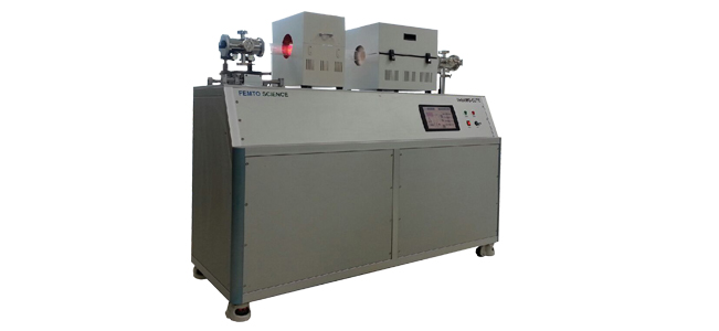
電漿反應系統 Femto Science CVD Graphene 腔體尺寸: 55 Dia. × 1300 L, mm 腔體溫度: 最高1200˚ C 功率: 300W, 20 – 100 KHz 控制器: 7吋觸控面板,自動/手動控制 設備尺寸: 1750 × 700 × 1200 (W × D × H, mm) 選配套件: 300W RF產生器
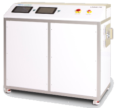
電漿反應系統 Femto Science Coating System 水平式腔體: 203 Dia. × 440 L, mm 垂直式腔體: 300 Dia. × 400 L, mm 蒸發器溫度: 最高200˚ C 腔體溫度: 最高1000˚ C 控制器: 7吋觸控面板,自動/手動控制 設備尺寸: 1500 × 800 × 1180 (W × D × H, mm)
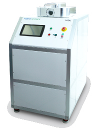
電漿反應系統 Femto Science Etching System 電漿蝕刻系統 腔體尺寸: 9.2英吋 功率: 300W, 13.56 MHz 氣體管路: 最多6組 控制器: 7吋觸控面板,自動/手動控制 設備尺寸: 680 × 1100 × 1300 (W × D × H, mm)
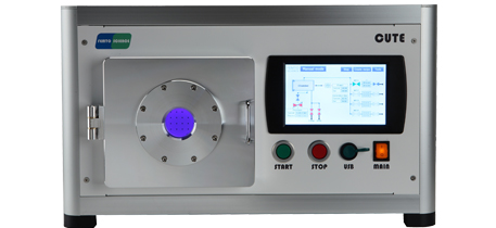
電漿反應系統 Femto Science Surface Treatment 表面處理設備 設計精美,多種腔體尺寸及功率可供選擇,可加裝石英反應管,最高支援6組氣體管路。全面配備7吋觸控面板,可全自動系統控制。 腔體尺寸: 140 × 200 × 110 (W × D × H, mm) 功率: 100W, 20 – 100 KHz 控制器: 7吋觸控面板,自動/手動控制 設備尺寸: 580 × 580 × 340 (W × D × H, mm) 腔體尺寸: 200 × 220 × 160 (W × D × H, mm) 功率: 200W, 20 – 100 KHz 控制器: 7吋觸控面板,自動/手動控制 設備尺寸: 618 × 630 × 460 (W × D × H, mm) 腔體尺寸: 330 × 350 × 250 (W × D × H, mm) 功率: 300W, 20 – 100 KHz 控制器: 7吋觸控面板,自動/手動控制 設備尺寸: 780 × 760 × 800 (W × D × H, mm) 選配套件: 石英管(200 Dia. × 300 L, mm)、RF產生器(300W) 腔體尺寸: 客製化 功率: 最高2000W, 20 – 100 KHz 控制器: 7吋觸控面板,自動/手動控制 氣體管路: 最多6組 選配套件: 石英管、RF產生器
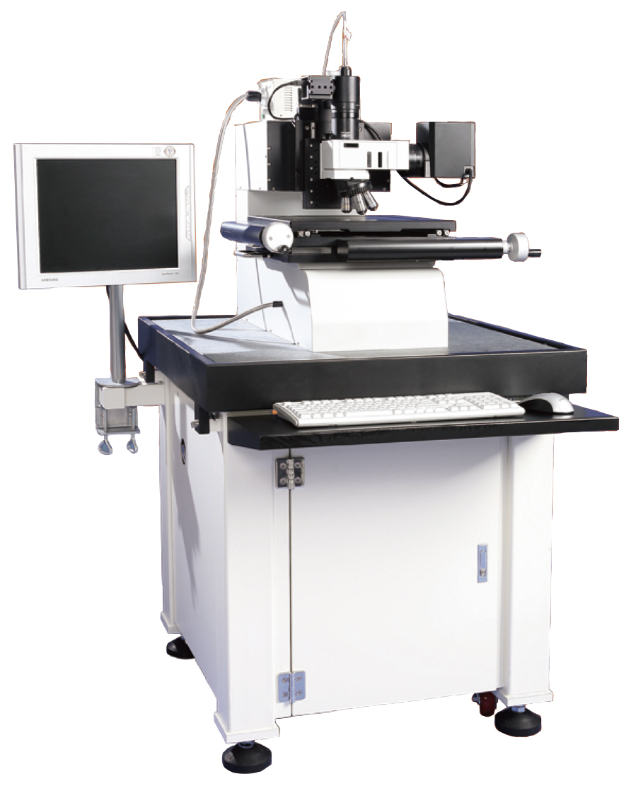
光譜式模厚量測儀 Ellipso Technology Elli-RSc (Reflectometer) 光譜式反射儀 高速膜厚量測系統,1秒鐘內完成單點量測(依材料性質而異)。最高可量測3層薄膜(依材料性質而異),厚度範圍10nm – 50mm(依材料性質而異)。配備顯微鏡系統,光點大小可調整,適用於半導體、OLED、高分子、太陽能…等相關研究及材料厚度檢測。 系統特性 光源波長範圍: 450nm – 900nm 光點大小: 50mm、30mm、10mm 量測層數: 最多3層(依材料性質而異) 量測厚度範圍: 10nm – 50mm (依材料性質而異) 再現性: ± 1 Å 載台尺寸: 140mm x 130mm 可加裝單波長雷射激發光源 應用: OPTION Thick film measurement system : thickness range 1.0 ~ 300 um (mFFT*) Beam spot size : 4.0 um Stage size : 200 x 200 mm^2, 300 x 300 mm^2 and others (ask for a customized stage size) Auto focusing system : Color CCD camera Anti-vibration table Transmittance module 型錄下載
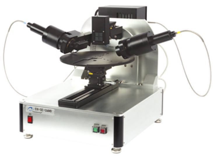
光譜式模厚量測儀 Ellipso Technology Elli-SE 光譜式橢圓偏振儀 高效能膜厚量測系統,最高可量測10層薄膜(依材料性質而異),單層厚度sub Å – 10mm(依材料性質而異)。非破壞性、高解析度且量測時間短,適用於半導體、OLED、高分子、太陽能…等相關研究及材料厚度檢測。 系統特性 光源: 氘燈 + 鹵素燈 入射角: 55˚ – 90˚ 光點大小: 1.5mm 量測層數: 最多10層(依材料性質而異) 量測厚度範圍: sub Å – 10mm(依材料性質而異) 再現性: ± 0.3 Å 載台尺寸: 6英吋 選配功能: CCD數位相機(影像觀測)、XY自動掃描載台、12英吋樣品載台、5秒快速量測套件(因材料性質而定) 應用: Semiconductor : Si, Ge, ONO, ZnO, AZO, PR, poly-Si, GaN, GaAs, Si3N4 Display(incl. OLED) : MgO, ITO, PR, NPB, Alq3 , CuPc, PVK, PAF, PEDT-PSS Dielectrics : SiO2, TiO2, Ta2O5, ITO, AIN, ZrO2, Si3N4, Ga2O3, Wet oxides Polymer : Dye, NPB, MNA, PVA, PET, TAC, PR Chemistry : Organic film(OLED) & LB Thin film Solar cell : SiN, a-Si, poly-Si, SiO2, Al2O3 型錄下載
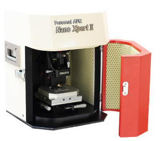
Nano Xpert II原子力顯微鏡(Atomic Force Microscopy, AFM) 個人化桌上型AFM系統,可搭配各廠牌之探針,體積小、不占空間,模組化軟硬體設計搭配快速校正程序,初學者也能輕易上手。 簡易操作程序 磁吸式探針座,搭配高倍率顯微鏡及高解析度觀測攝影機,非專業操作人員亦可快速進行雷射訊號校正。 高解析度影像 XY軸掃描控制器提供VCM type與PZT type兩種選擇,最大掃瞄範圍200mm × 200mm(VCM type,選配),最高解析度可達0.2nm。Z軸方向配備PZT type掃描控制器,最大掃瞄範圍7 mm,解析度可達0.02nm。另可選配30mm × 30mm電動平移載台,提升操作便利性。 整合式操作軟體 提供Contact、NonCantact、Tapping與Lateral Force種量測模式,直覺化軟體操作介面,只需簡單的參數設定即可開始進行掃描。另外整合AFM分析軟體,提供快速的影像處理與數據分析。 產品規格 操作軟體: 應用:
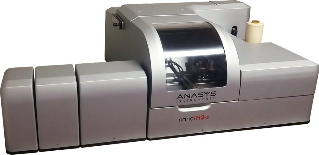
業界唯一,結合AFM-IR與s-NSOM之材料與生物科學分析設備。nanoIR2-s包含完整AFM功能,再加上高解析度的AFM-IR光譜以及s-NSOM的光學性質量測,提供前所未見的材料分析平台。 主要功能: 應用:
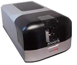
最新一代奈米級紅外線光譜儀,最高解析尺度達10nm。nanoIR2-FS所量測之紅外線圖譜與穿透式FTIR光譜直接相關,將紅外線光譜於材料分析領域拓展至嶄新的層次。 - 高速、高解析度之AFM-IR圖譜,只需數秒的時間即可完成光譜掃描 - 最高10nm光譜影像解析度 - AFM-IR圖譜等同FTIR光譜,可直接進行比對分析 - 完整的AFM掃描功能,表面型態與化學組成同時解析 - 搭配ThermaLeverTM 探針,可量測玻璃轉移溫度、熔點…等性質,將材料的熱分析提升至奈米級尺度。 產品功能: 應用:
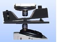
MultiView 1000 Entry-level system with optical capability upgrade The award winning MultiView 1000TM is an entry-level system that fully integrates all forms of scanning probe microscopy (SPM) with conventional optical microscopy. The MultiView 1000 system provides a cost-effective SPM solution complete with advanced SPM features. The design of the MultiView 1000 emphasizes ease-of-use so that customers with any technical background can quickly make SPM measurements. This system can also be easily upgraded to more sophisticated measurements such as NSOM and AFM-Raman. MV 1000 Product brochure can be downloaded here Unprecedented flexibility and performance Ease of use designed for quick setup with any background. Compatible with NanoToolKit of probes including all third party silicon probes. Easily upgradable to perform sophisticated measurements including AFM-Raman and NSOM Standard packages include magnetic force microscopy (MFM) and electrostatic force microscopy (EFM); more advanced modes including kelvin force microscopy and scanning capacitance microscopy available in an upgrade Complete optical access to scanning probe microscopy head Unique geometry leaves the optical axis free both above and below the sample for integration with upright, inverted, and dual optical (both upright and inverted) microscopy configurations Accomodates wide variety of probes Nanonics provides a wide variety of probes that are compatible with the MultiView 1000 including glass, cantilevered probes, thermal probes, electrical and magnetic probes (electrochemical probes, coax probes, glass insulated wire probes), all third party silicon probes, chemical writing probes Largest Commercially Available Z Scan Range The large 85 micron x,y, and z-range of the Nanonics 3D Flatscan makes it ideal for optical sectioning in confocal imaging. Used in this way, the MultiView 1000 integrates conventional far-field imaging, confocal microscopy, AFM, and near-field optics in a single system. Overall, the MultiView 1000 is a robust and versatile SPM system that allows the user to zoom, with overlapping fields of view, from the lowest resolution of conventional far-field imaging to the higher resolution of confocal microscopy, and finally, to the ultimate resolution of AFM and NSOM.
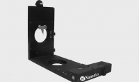
Advanced, Fully Featured SPM The MultiView 2000TM series is an advanced single probe scanning probe microscope enabling a variety of modes of AFM/SPM/NSOM imaging. Nanonics has designed The MultiView 2000TM for excellence in scanning probe microscopy while allowing for near-field and far-field optical NSOM/AFM Raman/TERS imaging without perturbation. The Multiview 2000TM is the only commercially available instrument that offers both tip and sample scanning. This versatility is important for different operation modes where the user can now choose whether the sample or tip is static. The Multiview 2000TM further offers the most stable feedback mechanism available in the form of normal force feedback with tuning fork actuation. This feedback mechanism offers the most stability, as well as laser-free operation for the most sensitive experiments. The MV 2000TM product brochure can be downloaded here. Designed for Ease-of-Use and Flexibility Dual sample and tip scanning stages in the same head for ultimate flexibility is coupled with an optically friendly Nanonics 3D Flat ScanTM stage providing up to 85μ in X, Y and Z or 170μ in X, Y and Z using combined scanners. This scanner is also suitable for large samples with unconventional geometries. Closed loop is an option for positioning accuracy of 20nm. Additionally, a revolutionary, alignment-free feedback system provides the most sensitive tip-sample stability. Normal force feedback with tuning fork actuation provides no alignment, laser-free operation for improved optical signal to noise ratio, and ultra-sensitive force spectroscopy perfect for force and adhesion measurements. Read more for more information and details about tuning fork feedback Largest Commercially Available Z Range The large, 85μ X, Y and Z-range of the Nanonics 3D FlatscanTM makes it ideal for optical sectioning in confocal imaging. Used in this way, the MultiView 2000TM integrates conventional far-field imaging, confocal microscopy, AFM, and near-field optics in a single system Excellent SPM platform compatible with wide variety of probes Nanonics provides a wide variety of probes that are compatible with the MultiView 2000TM, including: transparent, cantilevered probes, thermal probes, electrical probes (electrochemical probes, coax probes, glass insulated wire probes) and all third party silicon probes Any Optical Configuration The unique geometry of the MultiView 2000TM head and cantilever probes leaves the optical axis free both above and below the sample for integration with upright, inverted, and dual optical microscope configurations. Irregular Sample Size Compatibility Irregular sample sizes, whether odd in shape or large in size, can be easily placed on the sample stage. The sample can even be suspended from the unobstructed flat scanning sample stage in order to examine the edges of the sample.
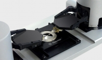
Up to 4 AFMs in One System • Four probes operate simultaneously and independently, with each probe having its own feedback and scanning capabilities. • Measure sophisticated properties only possible with the availability of multiple probes such as electrical, thermal and optical properties of devices • The MultiView 4000is a novel platform containing multiple probes/AFM's for advanced experiments such as: nanoscale transport, optical pump-probe, read-write experiments. The MV 4000 continues the tradition of the MV series of providing total optical flexibility and customization possibilities so that now AFM Raman and tip enhanced Raman spectroscopy (TERS) can be integrated with the multiprobe capability. Finally, free optical access from above allows easy visualization of all probes and facilitates nanomanipulation. The MV 4000 product brochure can be downloaded here. The simultaneous and independent SPM probe operation of up to 4 probes enables full characterization of all dimensions of samples and devices. All forms of SPM are enabled for each individual probe accompanied by total optical integration resulting in access to all modes including AFM, KPM, EFM, ANSOM, NSOM, STM, AFM-Raman, and TERS. Because these probes are designed for multiple probe operation, they can be brought to a nanometric separation distance thus ensuring that the same area is scanned with all the probes. Multiprobe capability is especially useful for electrical measurements since multiple probes can now be placed over the element to provide bias or probe its conductivity, resistance, etc just like in a probe station. Two-, three-, or four-point resistance measurements are possible. Multiple probes also enable flexible positioning and manipulation to provide bias, localized I-V measurements, and multichannel imaging. One probe can be the source of excitation while the second probe follows the transport process with high spatial resolution. Alternatively, optical pump/probe experiments can now be performed using one probe to optically pump while the other probe measures the optical output in a variety of configurations. An example of each type of measurement is shown below. Thermal transport measurement within an SRAM device where heat is introduced at specific locations and detected at other locations. As contact is made in different regions of the SRAM with the thermal conductivity probe, the probe tip cools to different levels depending on the material's thermal conductivity. The resulting image is obtained by determining the current alterations that had to to be affected in order to keep the current flowing past the point resistance at a constant value. With two cantilever, near-field optical probes with exposed tips, light is injected through one probe and is guided through the sample which is a fiber. With the second probe in place, this injected light can be collected and analyzed both spatially and temporally. In this image two NSOM probes are seen in AFM contact with the input and output of the fiber waveguide. See a video showing an example using multiprobe technology to conduct nanothermal measurements here. With a multiprobe system, resolution and tip quality no longer need to be compromised since each probe is now individualized for each measurement. In classic NSOM setups the NSOM probe would have the dual function of imaging topography and fluorescence where the topography image is compromised by the aperture (wider diameter) needed by the NSOM probe. But in a multiprobe setup, a standard SPM probe can be used the topography without affecting the NSOM fluorescence measurement. The left and center images are the topography and fluorescence images, respectively, of lumogen dye particles collected in a multiprobe setup with different probes for topography and NSOM. The image on the right is the topography image of the same sample but collected with the NSOM probe, revealing the clear loss of resolution and morphology. The width of each image is 8um. One probe can be used for moving, cutting, or positioning a sample, while the other probe can be used to image the sample. For example, shown below is a chromosome that has been dissected with one probe (see image on left), while the other probes images the result of the nanomanipulation. (Left) MultiView 4000TM four SPM probes platform. (Middle) MultiView 4000TM Tip and Sample scanning stages. (Right) Optical image of online four SPM probes in feedback. The images above show the procedure that can be implemented to bring two or more probes in close proximity to one another. Specifically in the images shown the common features in a carbon nanotube sample are imaged by two probes and from these images it is clear that the two probes are displaced along the y axis by 300nm and along the x axis by 1.7microns
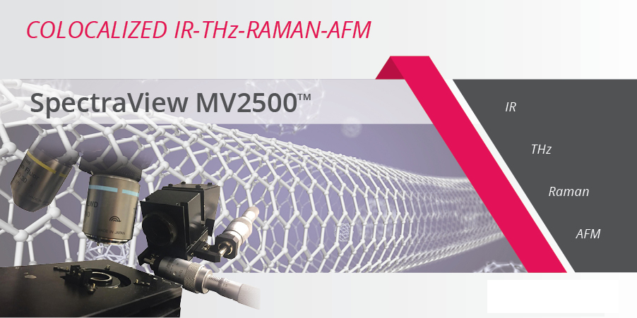
A Breakthrough in Combining Complementary Scattering Techniques with Ultrasensitive AFM and SPM for NanoChemical Analysis • Colocalized IR, Raman, THz and AFM • Singular protocols for excitation in the IR with Raman and fluorescence detection in the visible • Image with photon force with pN force sensitivity • Patented cantilevered completely transparent probes • Highly localized scattering at the tip • Versatile configurations with advanced SPM modes of operation: Kelvin Probe chemical potential, electrical, thermal and photon force detection • Online variable magnetic fields • Applications in plasmonics of 2D materials, liquids, biology etc. AFM (Left) and IR (right) images obtained with broadband IR illumination (1000-4000cm-1) at the MIRIAM beamline of the Diamond Light Source, Harwell, United Kingdom
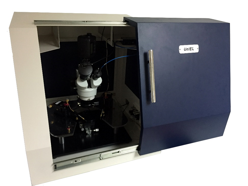
UniEL 電致發光光譜儀 以SZM series顯微鏡為主體,整合電源供應器、輝度計、光譜儀及觀測用數位相機,同步量測元件放射光之輝度及光譜分布,搭配專屬控制軟體,精準控制電流/電壓及訊號擷取,是光學元件開發必備工具。 產品特色: - 同步式輝度計 / 光譜儀 / CMOS Camera - Keithley Source Meter - Konica Minolta Luminance and Color Meter - 4-Way Electrode Probe - 5M Pixel CMOS Camera - 350nm – 1000nm Linear CCD Detector - Time resolution EL is available - In-situ luminance, spectrum and current(voltage) measurement
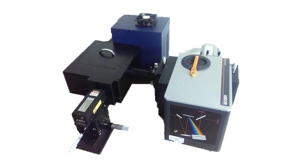
UniPLUX PL / TRPL / Upconversion 光譜儀 產品特色: - 可以量測需求選擇白光、雷射或脈衝式雷射作為激發光源 - 可選擇CCD或PMT偵測器 - 可搭配顯微鏡升級為微區螢光偵測系統 - 可進行PL / TRPL / Upconversion 分析
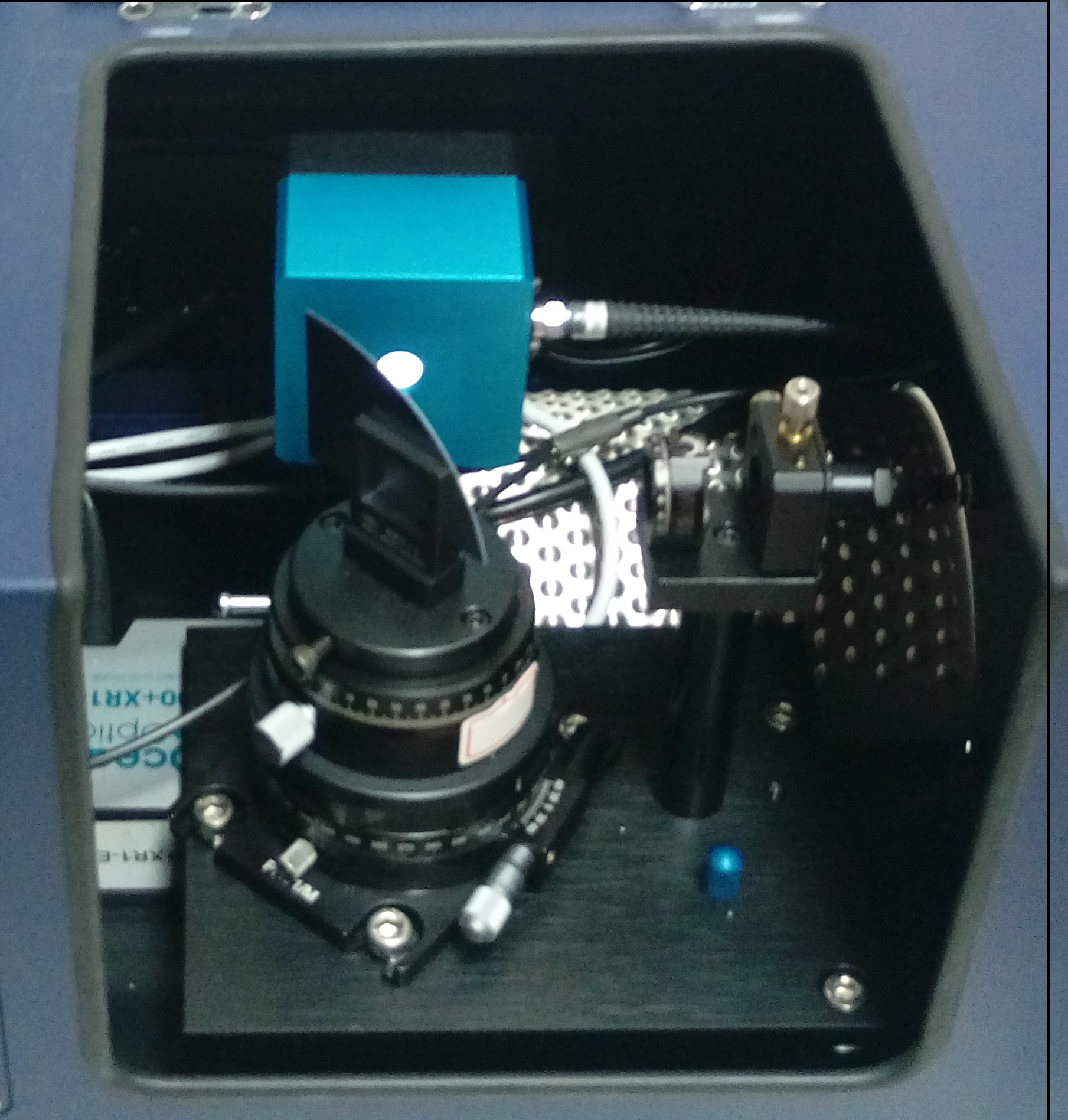
UniART 吸收/反射/穿透光譜儀 產品特色: - 內建白光激發光源 - 可選配雷射激發光源 - 偵測範圍200nm – 3000nm UV~NIR (需搭配不同偵測器) - 客製化樣品載具 - 可選配積分球與光源偏振片